Q 1>
(a) Explain the classification of smart materials.
ANS> Actively Smart:
They possess the capacity to modify their geometric or material properties under the application of electric, thermal or magnetic fields, thereby acquiring an inherent capacity to transduce energy.
• Piezoelectric
• Magneto strictive
• Shape memory alloys
• Electro-Rheological fluid, etc.
They can be used as force transducers and actuators
Passively Smart: Those smart materials that are not active are called passively smart materials. Although smart, they lack the inherent capability to transduce energy.
• Optic fibers
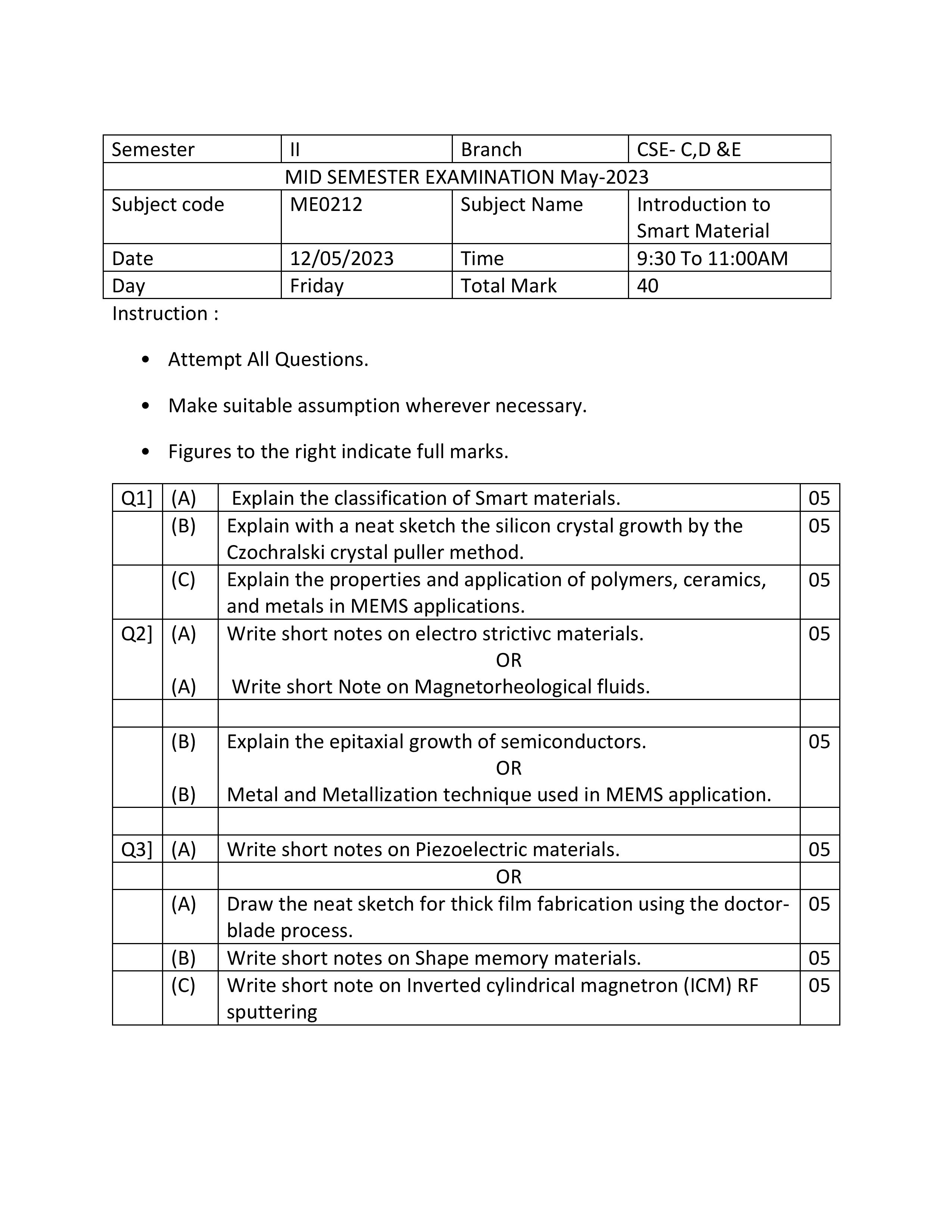
b) Explain with a neat sketch the silicon crystal growth by the Czochralski crystal puller method
ANS> • To demonstrate the methods of growing semiconductors, we will consider the crystal growth of silicon in detail first.
• Basically, the technique used for silicon crystal growth from the melt is the Czochralski technique.
• This starts from a pure form of sand (SiO2), known as quartzite, which is placed in a furnace with different carbon-releasing materials, such as coal and coke.
• Several reactions then take place inside the furnace and the net reaction that results in silicon is as follows:
• The silicon so-produced is known as metallurgical-grade silicon (MGS) which contains up to 2% of impurities.
• Subsequently, the silicon is treated with hydrogen chloride to form trichlorosilane (SiHCl3):
SiHCl3 is a liquid at room temperature. Fractional distillation of the SiHCl3 removes the impurities and the purified liquid is reduced in a hydrogen atmosphere to yield electronic- grade silicon (EGS) by the following reaction:
• EGS is a polycrystalline material of remarkably high purity and is used as the raw material for preparing high quality Si wafers. The Czochralski technique employs the apparatus shown in Figure 2.1.
• To grow a crystal, the EGS is placed in the crucible and the furnace is heated above the melting temperature of silicon. An appropriately oriented seed crystal (e.g. [100]) is suspended over the crucible in a seed holder.
• The seed is then lowered into the melt. Part of it melts but the tip of the remaining seed crystal still touches the liquid surface. The seed is next gently withdrawn, and progressive freezing at the solid–liquid interface yields a large single crystal.
• Absolute control of temperatures and pull rate is required for high quality crystals. A typical pull rate is a few millimeters per minute.
(c) Explain the properties and application of polymers, ceramics, and metals in MEMS applications
ANS> Polymers, ceramics, and metals are commonly used materials in Microelectromechanical Systems (MEMS) applications due to their unique properties and suitability for various purposes. Here’s an overview of their properties and applications
- Polymers:
- Properties: Polymers are organic compounds made up of long chains of repeating units. They exhibit excellent flexibility, low density, good chemical resistance, and electrical insulation properties.
- Applications: Polymers find applications in MEMS as flexible membranes, gaskets, coatings, and encapsulation materials. They are used in microfluidics devices, bioMEMS sensors, and actuators due to their compatibility with biological systems and ease of fabrication.
- Ceramics:
- Properties: Ceramics are inorganic, non-metallic materials characterized by their high hardness, excellent thermal stability, low thermal expansion, and electrical insulating properties. They are brittle and have high compressive strength.
- Applications: Ceramics are commonly used in MEMS applications where high-temperature stability, chemical resistance, and electrical insulation are required. They are used in pressure sensors, accelerometers, gyroscopes, and resonators. Ceramics such as silicon dioxide (SiO2) and silicon nitride (Si3N4) are frequently employed as structural materials and protective coatings.
- Metals:
- Properties: Metals possess high electrical conductivity, good thermal conductivity, high mechanical strength, and ductility. They can be easily formed, machined, and joined.
- Applications: Metals are widely used in MEMS for various applications. They are utilized in microfabricated devices such as microactuators, microcantilevers, and microvalves. Common metals used include gold (Au), aluminum (Al), copper (Cu), and nickel (Ni). Metal alloys like nickel-titanium (NiTi) shape memory alloys are employed for their unique shape-changing properties.
Q 2>a) Write short notes on electro strictive materials
ANS> Electrostrictive materials are a class of materials that exhibit a change in shape or size when subjected to an electric field. Similar to piezoelectric materials, electrostrictive materials undergo a mechanical deformation in response to an applied electric field. However, in contrast to piezoelectric materials, the deformation in electrostrictive materials is primarily due to the reorientation of electric dipoles within the material, rather than the displacement of charges.
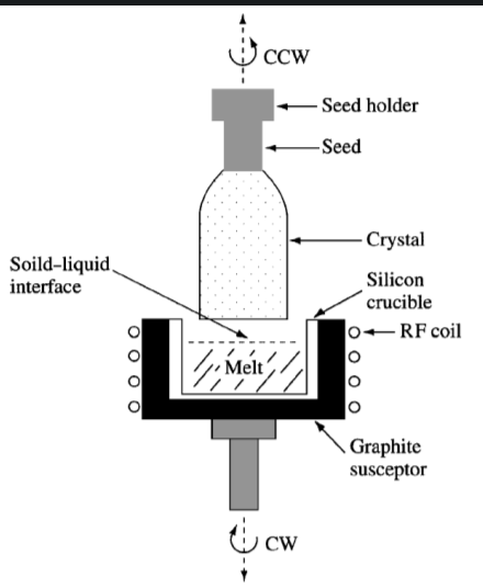
a) Write short non Magnetorheological fluids.
ANS> A MR fluid is a smart fluid which usually consists of 20-40 percent iron particles, suspended in mineral oil, synthetic oil, water or glycol.
- MRF also contains a substance which prevents the iron particles from setting.
- When subjected to a magnetic field, the magnetic particles inside increase the fluid’s viscosity, rendering it viscoelastic solid.
- “OFF” position – the MR fluid is not magnetized & the particles inside, distributed randomly, allow the fluid to move freely, acting like a damper fluid.
- “ON” position – the particles become energized and align into fibrous structures and restricts the movement of the fluid.
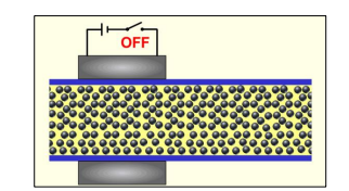
(b) Explain the epitaxial growth of semiconductors.
ANS> In many situations, it may not be feasible to start with a silicon substrate to build a smart system.
- Instead, one could start with other possibilities and grow silicon films on the substrate by epitaxial deposition to ‘build the necessary electronics’.
- The method for growing a silicon layer on a substrate wafer is known as an epitaxial process where the substrate wafer acts as the seed crystal.
- Epitaxial processes are different from crystal growth from the melt in that the epitaxial layer can be grown at a temperature much lower than the melting point.
- Among various epitaxial processes, vapor phase epitaxy (VPE) is the most common.
- A schematic of the VPE apparatus and shows a horizontal susceptor made from graphite blocks.
- The susceptor mechanically supports the wafer and being an induction-heated reactor it also serves as the source of thermal energy for the reaction.
- Several silicon sources can be used, e.g. silicon tetrachloride (SiCl4), dichlorosilane (SiH2Cl2), trichlorosilane (SiHCl3) and silane (SiH4).
- The typical reaction temperature for silicon tetrachloride is 1200 C.
- The overall reaction, in the case of silicon tetrachloride, is reduction by hydrogen, as follows:
- SiCl4 (gas) + 2H2(gas) –>Si (solid) + 4HCl
- A competing reaction which occurs simultaneously is:
- SiCl4 (gas) + Si (solid) –> 2SiCl2(gas)
- silicon is deposited on the wafer, silicon is removed (etched).
- Therefore, if the concentration of SiCl4 is excessive, etching rather than growth of silicon will take place.
b) Metal and Metallization technique used in MEMS application
ANS> Any of a class of substances characterized by high electrical and thermal conductivity as well as by malleability, ductility, and high reflectivity of light is called metal.
- Metals are used in MEMS and microelectronics due to their good conductivities, both thermal and electrical.
- Metals are somewhat strong and ductile at room temperature and maintain good strength, even at elevated temperatures. Hence, they could also be used to form useful structures.
- While thin metal films have been used in IC chips for a long time thick metal film structures are required for some MEMS devices.
- Thick metal films are generally used as structural materials in MEMS devices or as mold inserts for polymers in ceramic micro-molding.
- Nickel, copper and gold can be electroplated to form these thick films, while three- dimensional stainless steel micro-parts can be fabricated by a process known as photo- forming.
- Metallization is a process whereby metal films are formed on the surface of a substrate.
- Metal films can be formed by using various methods, with the most important being physical vapor deposition (PVD).
- The latter is performed under vacuum by using either an evaporation or sputtering technique.
- In evaporation, atoms are removed from the source by thermal energy while in sputtering, the impact of gaseous ions is the cause of such removal.
- In addition to several elemental metals, various alloys have also been developed for MEMS.
- CoNiMn thin films have been used as permanent magnet materials for magnetic actuation.
- NiFe permalloy thick films have been electroplated on silicon substrates for magnetic MEMS devices, such as micromotors, micro-actuators, microsensors and integrated power converters.
- TiNi shape memory alloy (SMA) films have been sputtered onto various substrates in order to produce several well known SMA actuators.
- Similarly, TbFe and SmFe thin films have also been used for magnetostrictive actuation.
Q 3>(a) Write short notes on Piezoelectric materials.
ANS> Piezoelectric Material
- Materials that produce a voltage when stress is applied. (An applied mechanical stress will generate a voltage)
- Example: Quartz, BaTiO3, GaPO4
- The piezoelectric effect describes the relation between a mechanical stress and an electrical voltage in solids.
- In physics, the piezoelectric effect can be described as the link between electrostatics and mechanics.
- An LED is wired to a piezoelectric transducer. The LED briefly lights when the device is flicked & shows that electricity has been generated by stress and strain.
- The second generation of piezoelectric applications was developed during World War II. It was discovered that certain ceramic materials, known as ‘ferroelectrics’, showed dielectric constants up to 100 times larger than common-cut crystals and exhibited similar improvement in piezoelectric properties.
Reverse Piezoelectric effect
- An applied voltage will change the shape of the solid by a small amount (up to a 4% change in volume).
- Quartz watches, Piezoelectric US oscillator
Application of Piezoelectric effect
- In lighters or portable sparkers with a piezo fuze a sudden and strong pressure is used to produce a voltage. The spark then ignites the gas.
- A piezo motor is based on the change in mechanical shape of a piezoelectric material when an tension is applied. The material produces ultrasonic or acoustic vibrations and produces a linear or rotary motion.
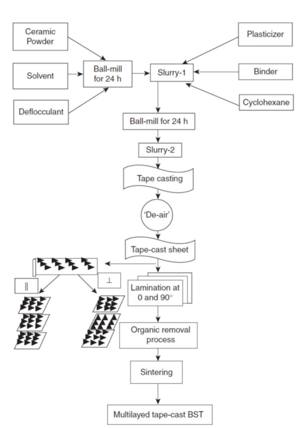
(a) Draw the neat sketch for thick film fabrication using the doctor-blade process .
ANS>
(b) Write short notes on Shape memory materials.
- ANS> An alloy that remembers” its original, cold-forged shape. By heating it returns back to the re-deformed shape.
- SMAs are materials which can revert back to original shape & size on cooling by undergoing phase transformations.
- Shape memory alloys (SMA’s) are metals, which exhibit pseudo-elasticity and the shape memory effect.
- Examples: NiTiNOL (thermal), NiMnGa, Fe-Pd, Terfenol-D (Magnetic) CuZnSi, CuZnAl, CuZnGa, CuZnSn(actuator)
- The shape change involves a solid-state phase change involving a molecular rearrangement between Martensite and Austenite.
- A temperature change of only about 100 C is necessary to initiate this phase change
- Shape Memory Alloys
A. Cu-based Alloys - Cu-Al-Ni with 14/14.5 wt.% Al and 3/4.5 wt.% Ni
- Cu-Sn approx. 15 at. % Sn
- Cu-Zn 38.5/41.5 wt.% Zn
- B. Other shape memory alloys include:
- Ni-Ti (~55% Ni)
- Ag-Cd 44/49 at. % Cd
- Au-Cd 46.5/50 at. % Cd
- Fe-Pt approx. 25 at. % Pt
- Mn-Cu 5/35 at. % Cu
- Fe-Mn-Si
- Pt alloys
- Co-Ni-Al
- Co-Ni-Ga
- Ni-Fe-Ga
(c) Write short note on Inverted cylindrical magnetron (ICM) RF sputtering
ANS> This consists of a water-cooled copper cathode, which houses the hollow cylindrical BST target, surrounded by a ring magnet concentric with the target.
A stainless steel thermal shield is mounted to shield the magnet from the thermal radiation coming from the heated table.
The anode is recessed in the hollow-cathode space. The latter aids in collecting electrons and negative ions, hence minimizing ‘re-sputtering’ the growing film.
Outside the deposition chamber, a copper ground wire is attached between the anode and the stainless steel chamber.
A DC bias voltage could be applied to the anode to alter the plasma characteristics in the cathode/anode space. The sputter gas enters the cathode region through the space surrounding the table.
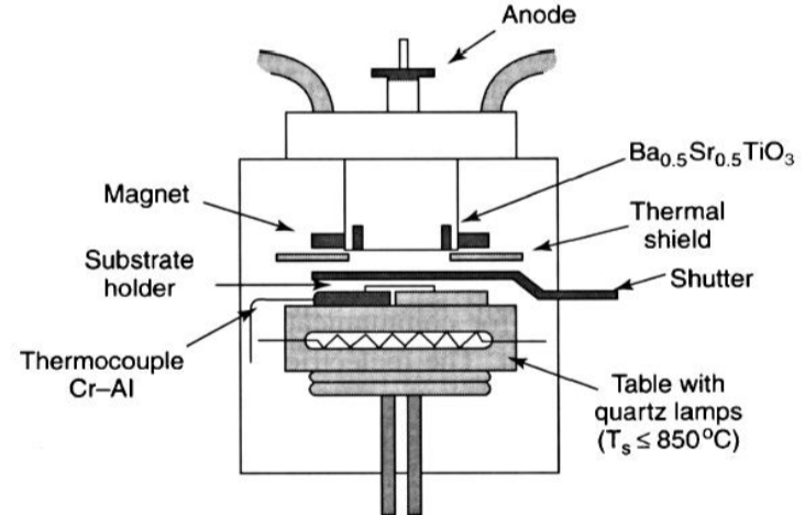
By using the above set-up, Cukauskas et al. were able to deposit BST films at temperatures ranging from 550 to 800 C.
The substrate temperature was maintained by two quartz lamps, a type-K thermocouple and a temperature controller.
The films were deposited at 135W to a film thickness of 7000A and cooled to room temperature at 1 atm of oxygen before removing them from the deposition unit.
This was then followed by annealing the films in 1 atm of flowing oxygen at temperature of 780 C for 8 h in a tube furnace.